持續創新改善 全員追求卓越
Continuous innovation and improvement
All employees pursue excellence

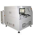


Semiconductor Industry
Laser marking /

-
Purpose of Use
Used in mass production lines to ensure cleaning consistency, yield, and stable production cycles, high-precision cleaning without damaging the substrate.
-
Main Purpose
Put into mass production, improve yield, reduce cleaning time, stabilize processes.
-
Laser Module
Uses high-stability laser source, supports custom energy curves and higher pulse repetition rates.
-
Optical System
High-end lens + custom spot optimization, adjusted for customer probe density/angle.
-
Fixture Design
Custom precision fixture (including angle compensation, high-precision X/Y/Z adjustment).
-
Processing Speed
Industry's fastest line scanning method, effectively improving processing speed.
-
Software Features
Complete interface: recipe management, point recording, history tracking, MES integration.
-
Automation Capability
Supports full automation: Tray loading/unloading, positioning camera, AI detection of contamination points.
-
Reliability
Designed for long-term mass production.
Product processing instruction
Other Product Description
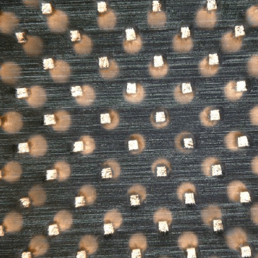
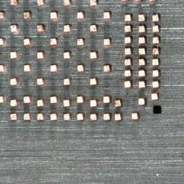
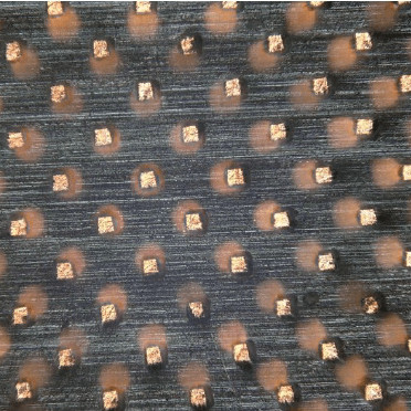 Before Processing - Central Area Probe (High Magnification Microscope)
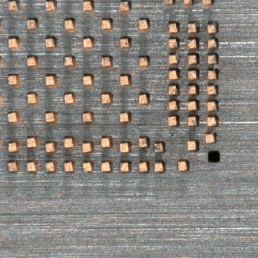
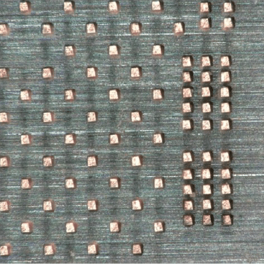
 After Processing - Central Area Probe Cleaning Excellent. Substrate Undamaged
 Before Processing - Lower Right Area Probe (High Magnification Microscope)
 After Processing - Lower Right Area Probe Cleaning Excellent. Substrate Undamaged
 Before Processing - Right Side Area Probe (High Magnification Microscope)
 After Processing - Right Side Area Probe Cleaning Excellent. Substrate Undamaged