持續創新改善 全員追求卓越
Continuous innovation and improvement
All employees pursue excellence
Cyber應用
Measuring the flatness of electronic components and wafers.
Product Description
Other Product Description
 FLATNESS MEASUREMENT
FLATNESS MEASUREMENT
- Measuring the flatness of electronic components and wafers
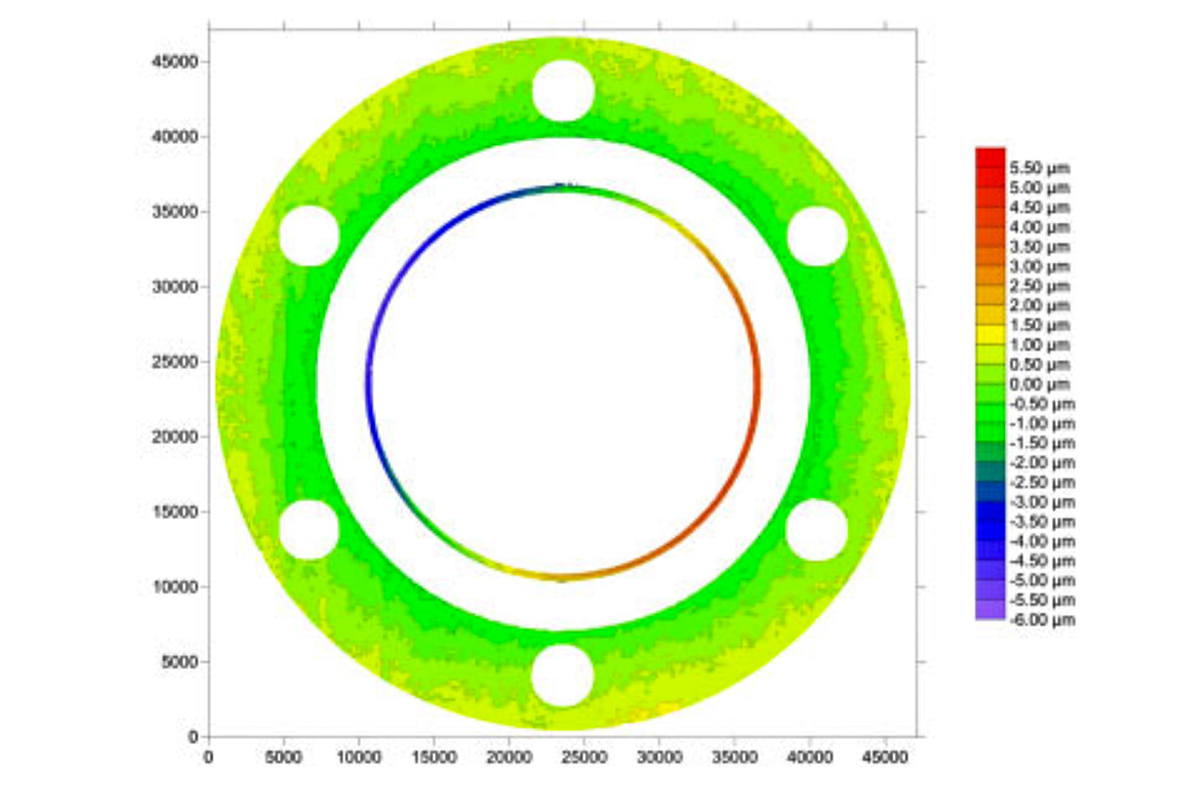
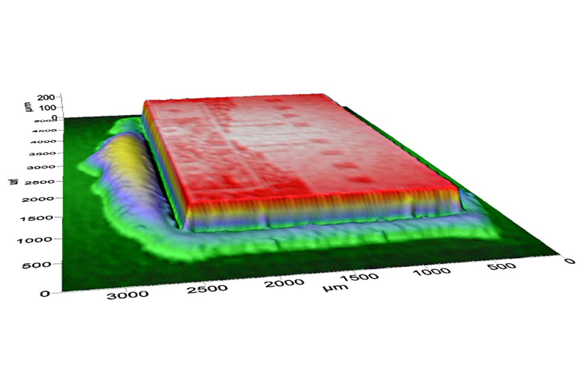
 ELECTRONIC COMPONENT
ELECTRONIC COMPONENT
- Countour map of an electronic component
- Advanced etch removing and modifiying algorithms
- Use polygon shape cursors to mark region of interest
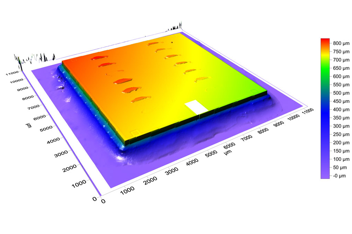
 HARD DISK DEVICE
HARD DISK DEVICE
- Contour map of hard disk device
- Effective filters to separate flatness from surface roughness
- Measuring the flatness relative to reference areas
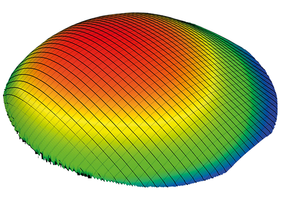
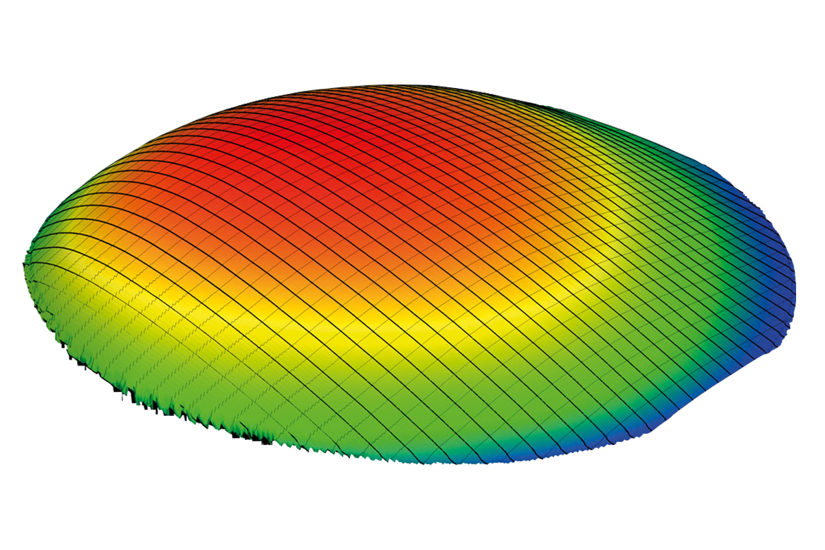
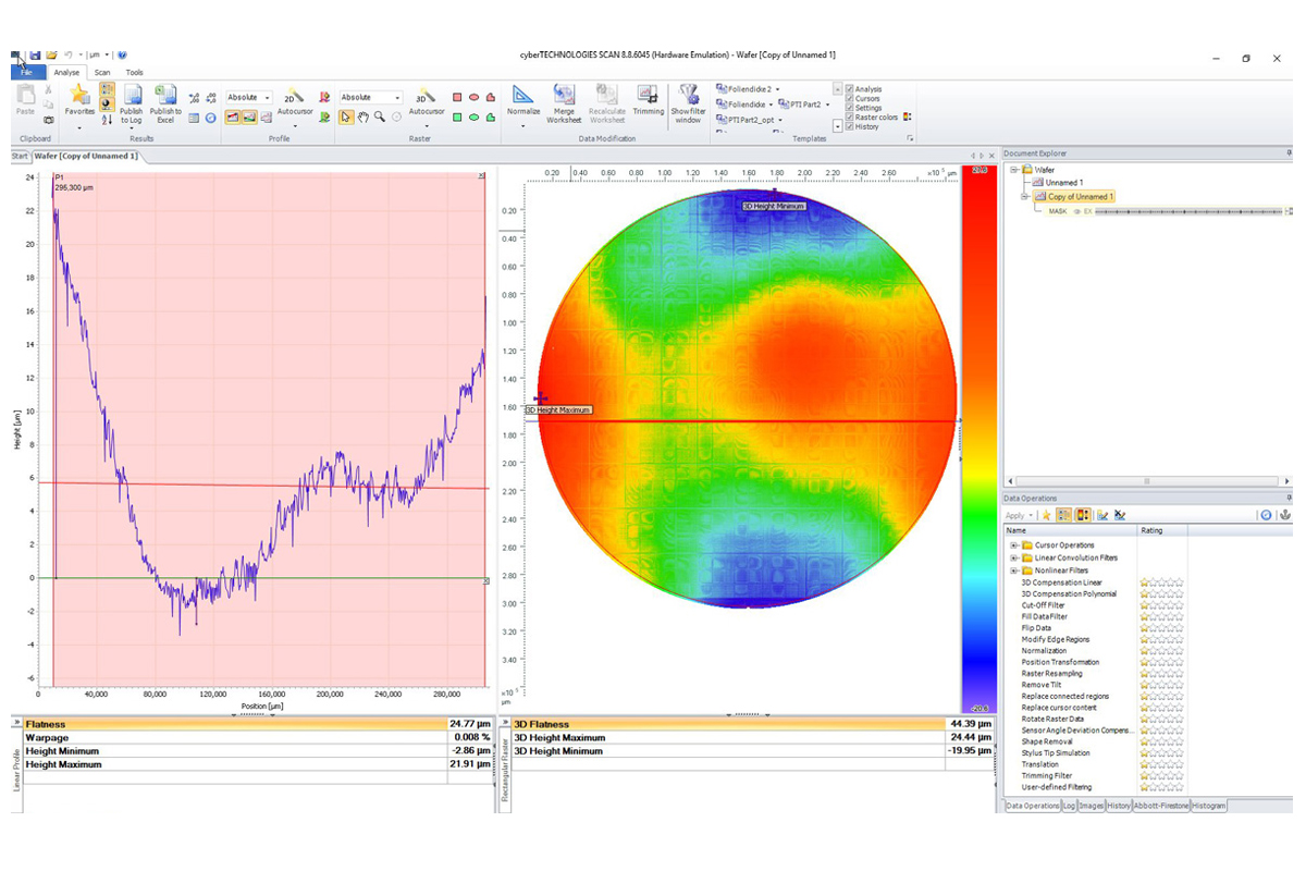 SURFACE OF A WAFER
SURFACE OF A WAFER
- Surface of a wafer
- Accurate flatness measurement over large areas
- Colors can be set to specification limits
 DIE TILT– LEADFRAME
DIE TILT– LEADFRAME
- 3D Image die tilt
- Measures Die Tilt, BLT height and Position
- Rotation and offset relative to cavity center