持續創新改善 全員追求卓越
Continuous innovation and improvement
All employees pursue excellence
Cyber應用
Measuring the thickness of various print layers on hybrid substrates
THICKNESS & THICKFILM
Controlling the thickness of various print layers on hybrid substrates is essential because electrical parameters are directly related to the thickness. cyberTECHNOLOGIES high resolution non-contact 3D measurement systems are the ideal tool for thickfilm measurements.
Product Description
Other Product Description
 THICKNESS & THICKFILM
THICKNESS & THICKFILM
- Measuring the thickness of various print layers on hybrid substrates.
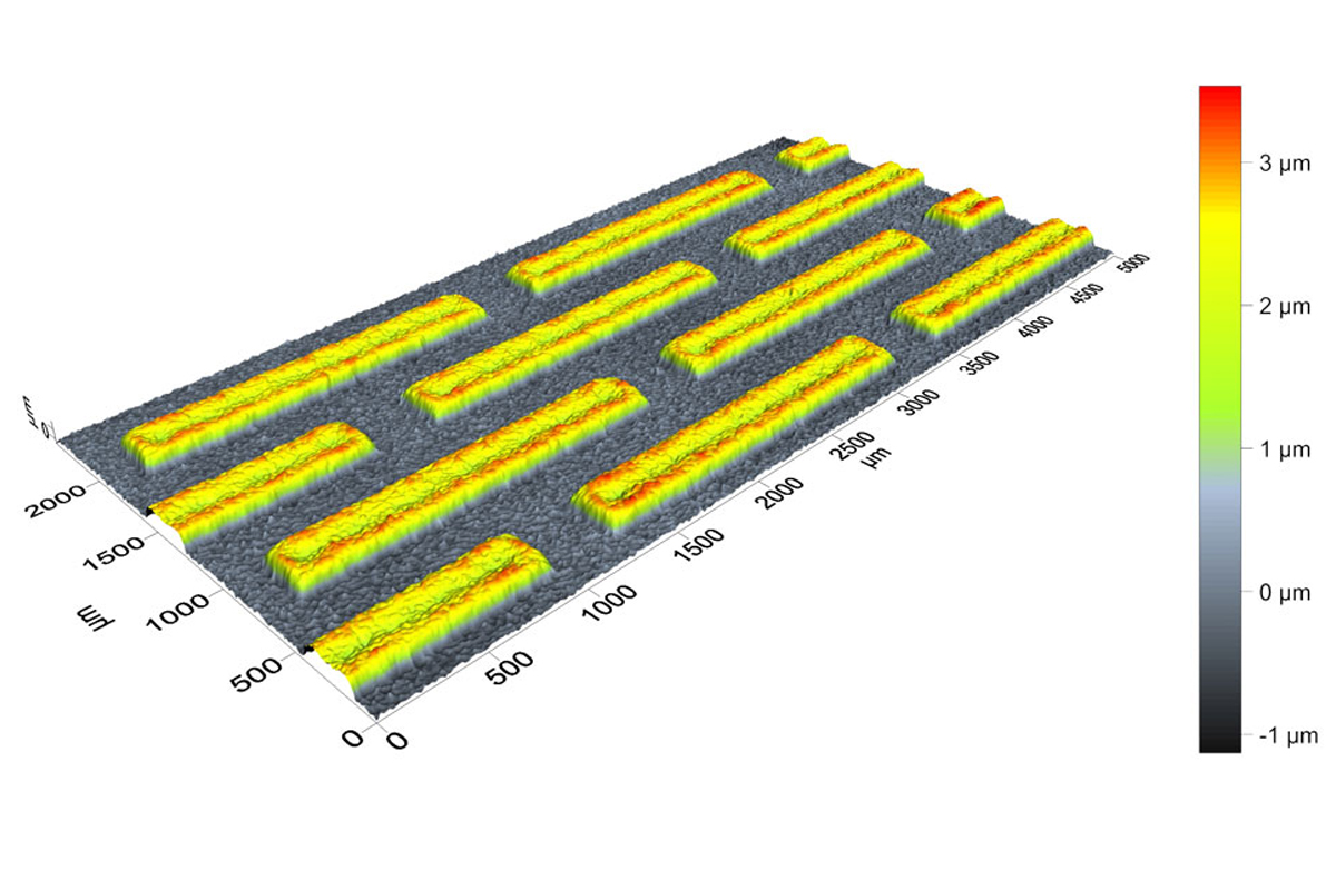
 HYBRIDCIRCUIT(1)
HYBRIDCIRCUIT(1)
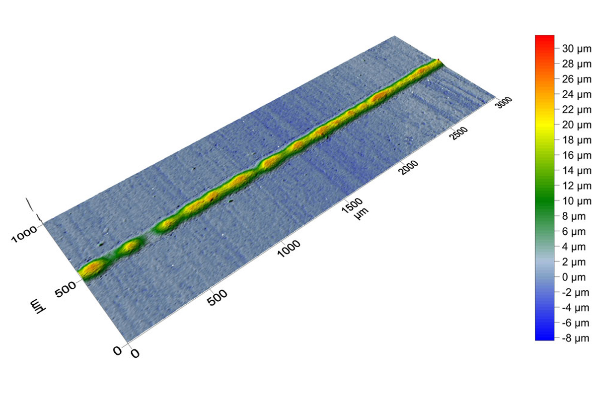
- Surface of a thick-film resistor
- Measurement of various layers like resistor-, silver-, gold- and glas prints
- View Surface and Contour Maps
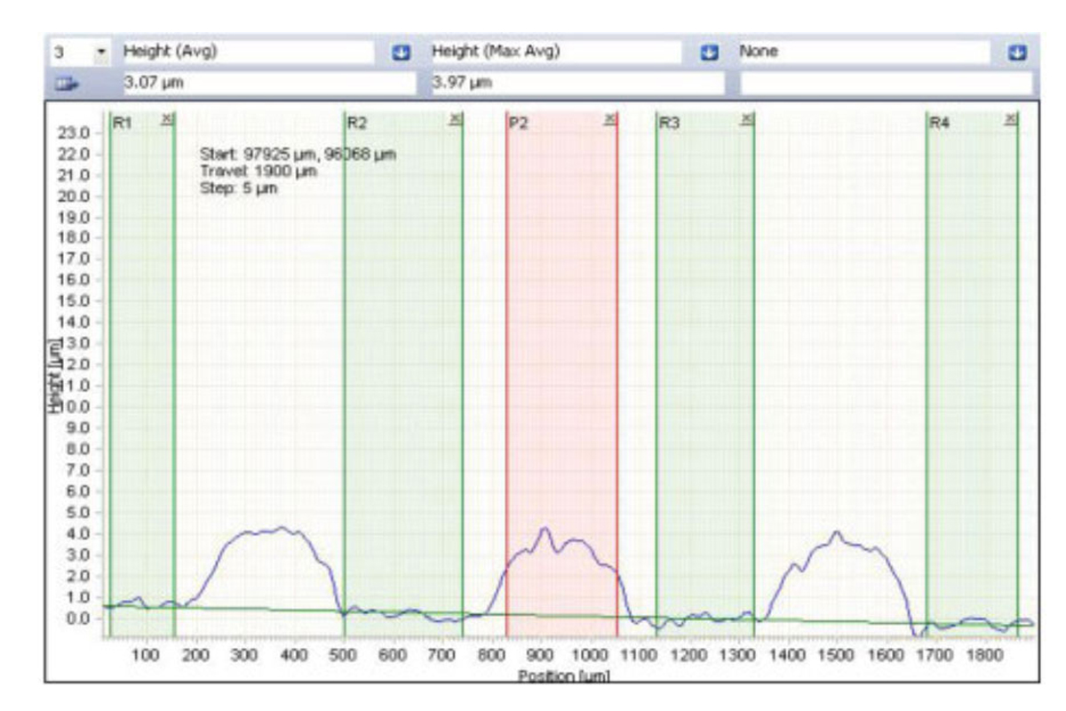
 HYBRIDCIRCUIT(2)
HYBRIDCIRCUIT(2)
- All sensors handle different surface reflections (ceramic – wet print)
- Height is measured using two or more reference cursors to compensate tilt or warpage
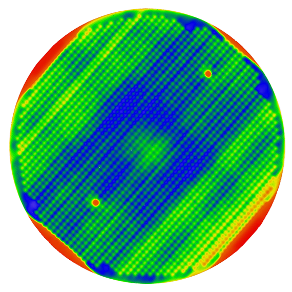
 SOLAR CELL(1)
SOLAR CELL(1)
- Surface of metallization layer
- Accurate 3D measurements are required to set-up and optimize the printing process
- Detect print variation on a single cell and from cell to cell
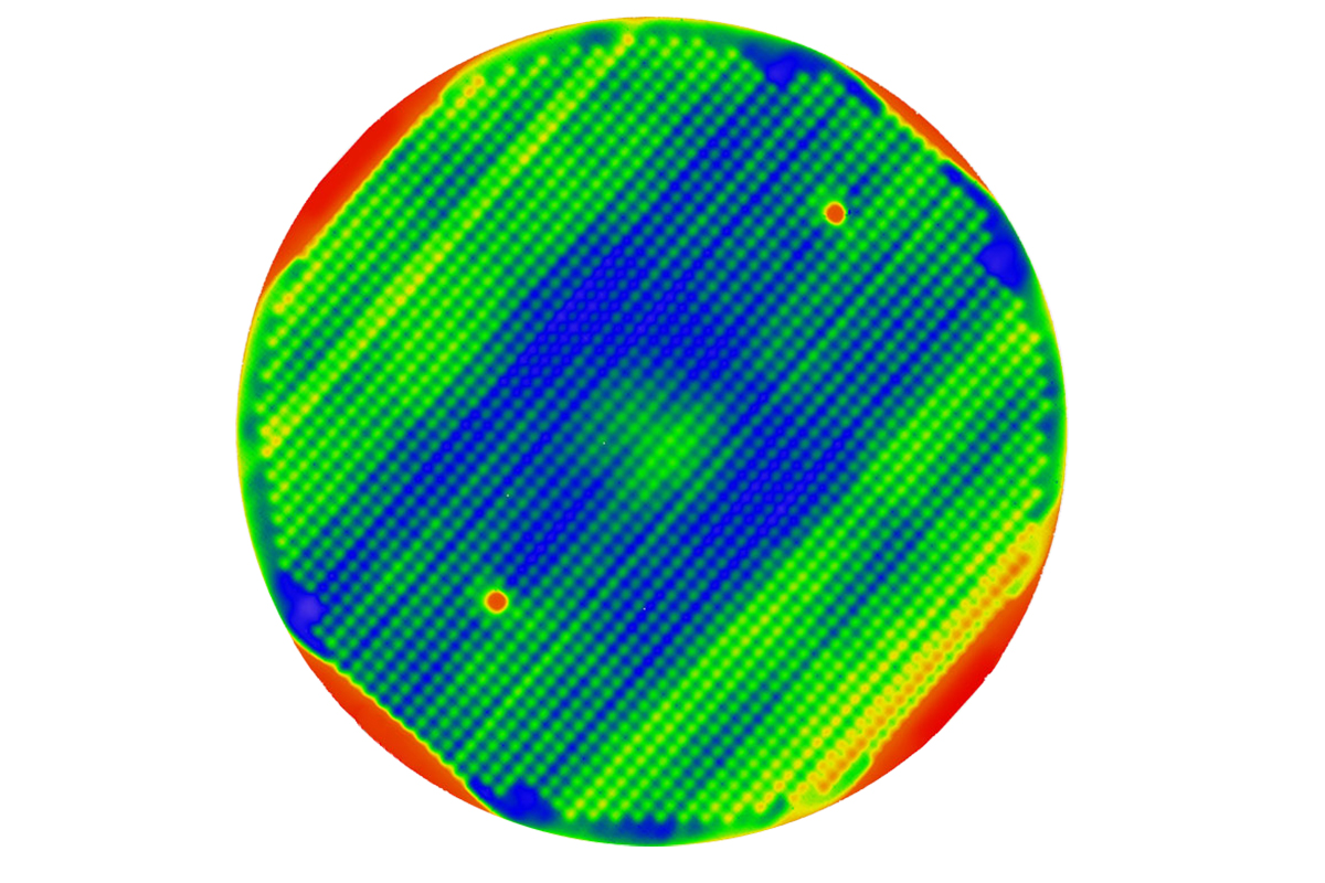
 SOLAR CELL(2)
SOLAR CELL(2)
- Profile of metallization layer
- “Blue Laser” can measure on texturized and coated wafers
- Solar Cell Measurement includes max height, average height and line width
 EPOXY PRINT(1)
EPOXY PRINT(1)
- Surface of printed and dispensed epoxy dots
- 3D volume, height and area measurements
- Report the position of the highest points of each deposit in an array
 EPOXY PRINTE(2)
EPOXY PRINT(2)
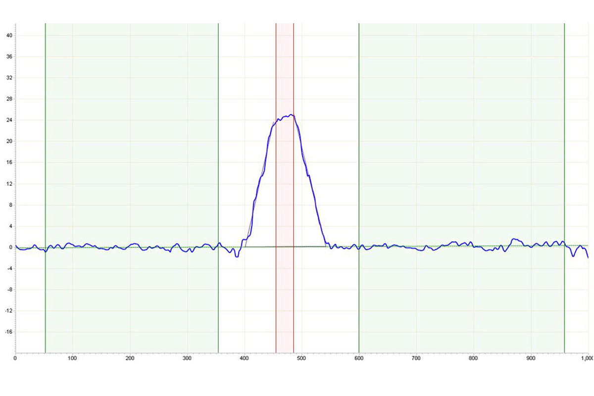
- Profile of an epoxy dot
- Measurement of transparent or translucent materials (solder mask, epoxy, flux etc.)
- Obtain several results in one setup (e.g. height, angle, length)
 MULTI-LAYER CERAMIC CAPACITOR (MLCC)(1)
MULTI-LAYER CERAMIC CAPACITOR (MLCC)(1)
- Surface of a MLCC print
- Lateral resolution down to 1 micron
- Accurate x and y measurements using 3D data
 MULTI-LAYER CERAMIC CAPACITOR (MLCC)(2)
MULTI-LAYER CERAMIC CAPACITOR (MLCC)(2)
- Profile of a print on a MLCC tape
- Thickness in sub-micron range is accurately measured
- Effective filter methods to separate roughness from surface features
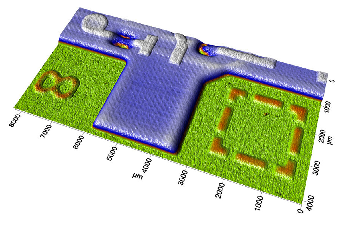
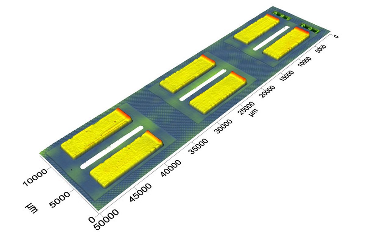
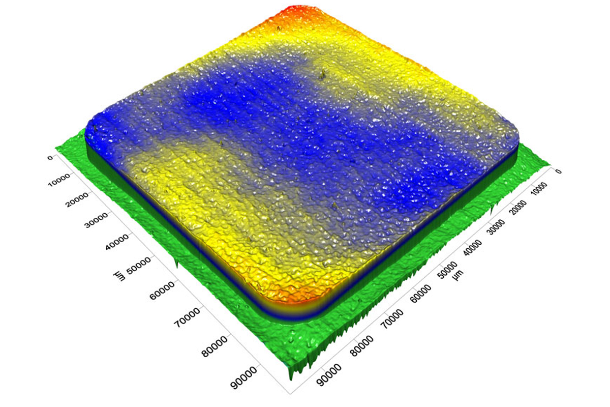 FUEL CELL(1)
FUEL CELL(1)
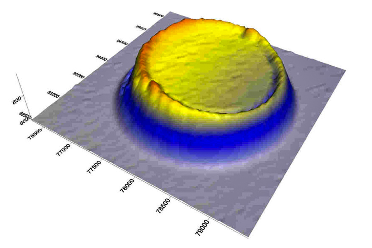
- Surface of a large print deposit on a fuel cell component
- Large scanning areas over the complete system travel
- Effective tilt and warpage compensation methods
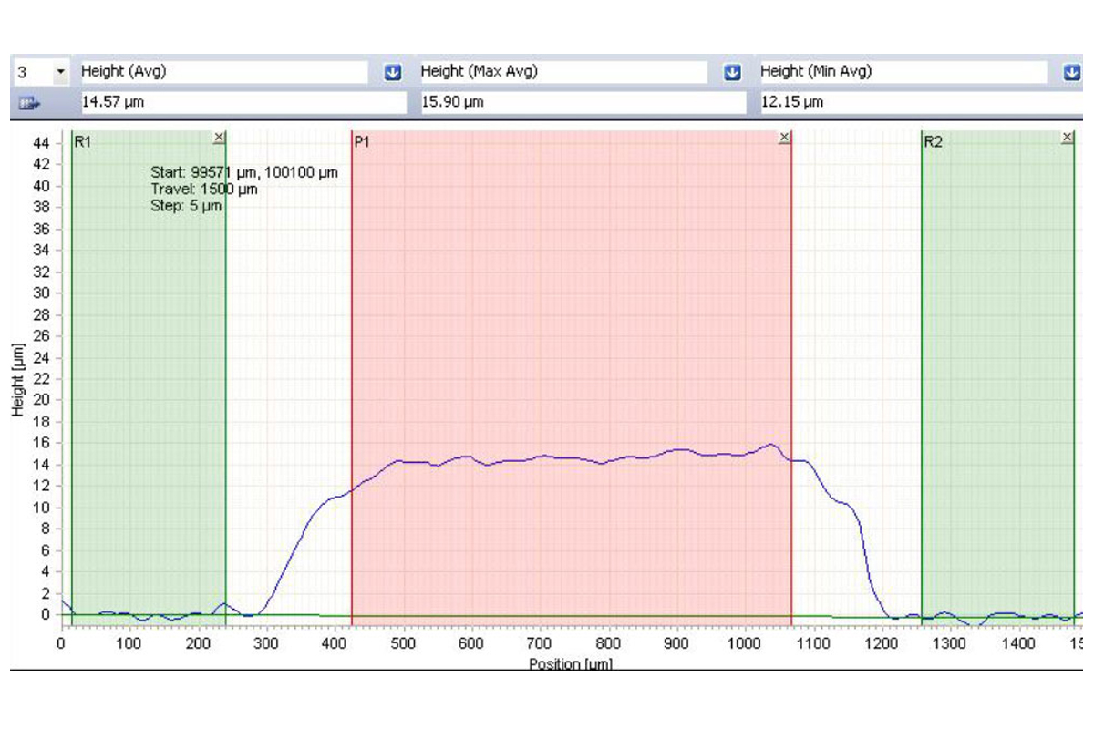
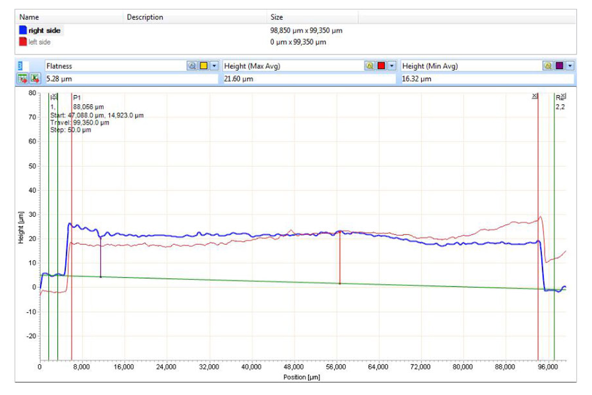 FUEL CELL(2)
FUEL CELL(2)
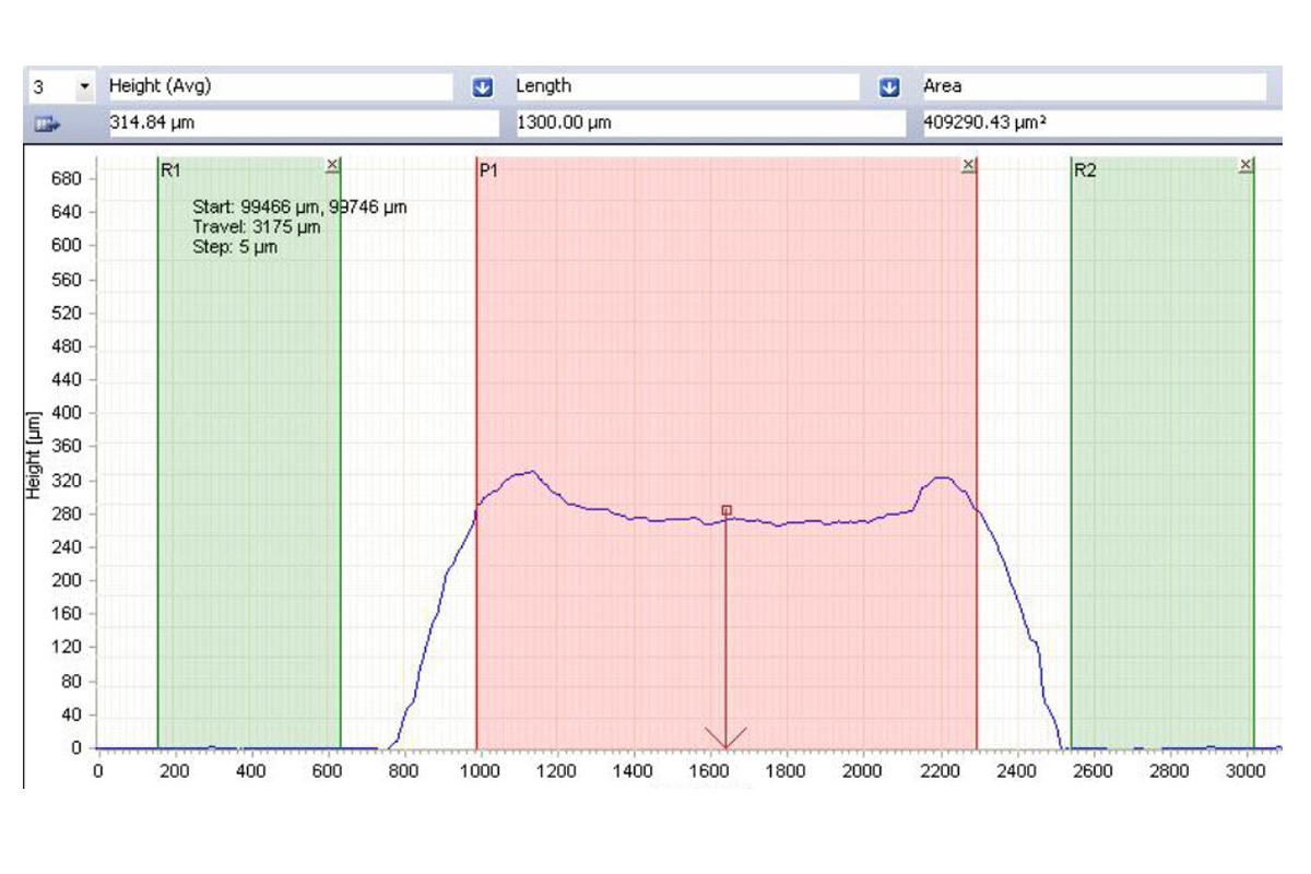
- Profile of a large print deposit on a fuel cell component
- Supports multiple worksheets in one document
- Overlay profiles from different positions
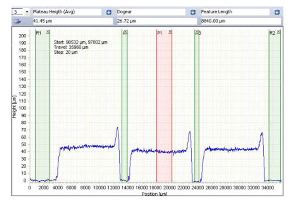
 DRAM EPOXY PRINT(1)
DRAM EPOXY PRINT(1)
- Profile of epoxy depots on a DRAM substrate
- Use several measurement and reference cursors to analyze multiple features in one scan
- Advanced print analysis: dogear, plateau height, plateau roughness, etc.
 DRAM EPOXY PRINT(2)
DRAM EPOXY PRINT(2)
- Profile of a print on a MLCC tape
- Thickness in sub-micron range is accurately measured
- Effective filter methods to separate roughness from surface features